


FOB Price
Get Latest Price0.1 ~ 3 / Piece ( Negotiable )
|1 Piece Minimum Order
Country:
China
Model No:
-
FOB Price:
0.1 ~ 3 / Piece ( Negotiable ) Get Latest Price
Place of Origin:
-
Price for Minimum Order:
0.1 per Piece
Minimum Order Quantity:
1 Piece
Packaging Detail:
Multilayer PCB package use vacuum packing and cartons package use vacuum packing and cartons
Delivery Time:
7~10 weekdays
Supplying Ability:
8500 Square Meter per Month
Payment Type:
T/T, L/C, D/A, D/P, Western Union, Money Gram, PayPal
Product Group :
-

China
Contact Person Ms. Tina
ShaJing, Shenzhen, Guangdong
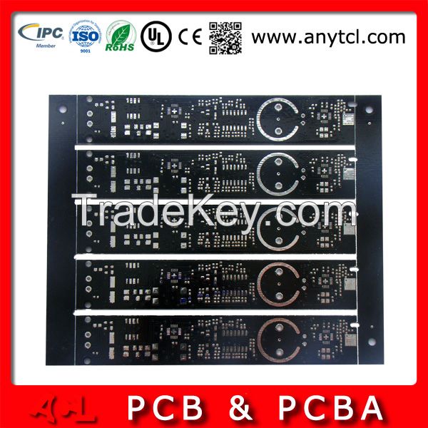
Multilayer PCBCapability Parameter:
| No | Item | Speccification |
| 1 | PCB Layers | Mass production:2~*8layers / Poilt run :*4Layers |
| 2 | Board thickness | 0.2mm~0.3mm |
| 3 | Copper Thickness | 0.5OZ~4OZ |
| 4 | Surface Finishing | HASL,Immersion Gold,Immersion Tin,OSP,OPS+ENIG,Immersion Silver,ENEPIG,Gold Finger |
| 5 | Gerber files | Gerber file or other pcb file is acceptable |
| 6 | Min.Hole size | Mechanical drill:0.2mm Laser drill : 0.**5mm |
| 7 | Min.Line Width | 0.1mm |
| 8 | Min.Line Spacing | 0.1mm |
| 9 | Min.Solder Mask Clearance | 0.**6mm |
| *0 | Min.Annular Ring | 0.**6mm |
| *1 | Max.Panel Size | ***0mm***0mm |
| *2 | Max.Copper Thickness | UL certificated:6.0 OZ / Polit run :*2 OZ |
| *3 | Profile and V-Cut | V-Cut, Jump V-Cut, CNC V-Cut, CNC-Routing, Stamping and Believeing |
Our team can provide you with the mulitlayer PCB layout services you need to get your projects done - and on schedule!
Why choose Anytech?
Our pcb layout team can do a complete layout project and help with
smaller portions such as placement studies, routing, generating
proper manufacturing files, library management, and so on. We
are happy to make small changes or complete large complex designs
or manfacture.
We understand that our customers often need a Multilayer
PCB design completed quickly. We support our customers
by providing expedited PCB layout service at no additional hourly
cost.
We provide quotes on an hourly basis (time and materials) or with a
fixed price. Call us today to find out how we can improve your
design quality, meet your deadlines, and save money.
Anytech offers the fastest turnaround to reach the prototype stage,
followed by quick transition to production and volume
manufacturing.
Testing Procedures For
Mulitlayer PCB Board
We perform multiple quality assuring procedures before shipping out any PCB board. These include:
Visual Inspection
Flying probe
Bed of nails
Impedance control
Solder-ability detection
Digital metallograghic microscope
AOI (Automated Optical Inspection)
X-RAY
Detailed Terms for PCB board
Manufacturing
Technical requirement for pcb
board and assembly
Professional Surface-mounting and Through-hole soldering Technology
Various sizes like ***6,***5,***3 components SMT technology
ICT(In Circuit Test),FCT(Functional Circuit Test) technology.
PCB Assembly With UL,CE,FCC,Rohs Approval
Nitrogen gas reflow soldering technology for SMT.
High Standard SMT&Solder Assembly Line
High density interconnected pcb
board placement technology capacity.
Delivery Time for PCB board
1) PCB board
production time: sample: **4 days / mass production: within 7 days
2) Component purchase: 2 days if all components is available in our domestic market.
3) PCB board and
Assembly: samples: whthin 2 days / mass production: within 5 days
Shipping Method and Payment terms
for pcb board:
1. By DHL, UPS, FedEx, TNT using clients account.
2. We suggest you using our DHL, UPS, FedEx, TNT forwarder.
3. By EMS (Usually for Russia Clients), price is high.
4. By sea for mass quantity according to customer's requirement.
5. By customer's Forwarder
6. By Paypal, T/T, West Union,
etc.
Any needs or questions ,please contact
me! :)
| Country: | China |
| Model No: | - |
| FOB Price: | 0.1 ~ 3 / Piece ( Negotiable ) Get Latest Price |
| Place of Origin: | - |
| Price for Minimum Order: | 0.1 per Piece |
| Minimum Order Quantity: | 1 Piece |
| Packaging Detail: | Multilayer PCB package use vacuum packing and cartons package use vacuum packing and cartons |
| Delivery Time: | 7~10 weekdays |
| Supplying Ability: | 8500 Square Meter per Month |
| Payment Type: | T/T, L/C, D/A, D/P, Western Union, Money Gram, PayPal |
| Product Group : | - |


")


 2 layers-10 layers")