Product Description
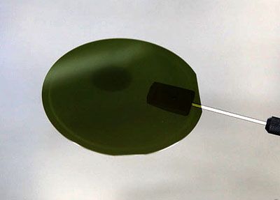
Helios provides high quality SiC wafer (Silicon Carbide) to
electronic and optoelectronic industry . SiC wafer is a next
generation semiconductor material, with unique electrical
properties and excellent thermal properties , compared to silicon
wafer and gallium arsenide wafer , SiC is more suitable for high
temperature and high power device.
SiC Wafer Features :
• Low lattice mismatch
• High thermal conductivity
• Low power consumption
• Excellent transient characteristics
• High band gap
SiC Wafer Application :
• GaN epitaxy device
• Optoelectronic device
• High frequency device
• High power device
• High temperature device
• Light emitting diodes
Regular specification of SiC Wafer
Polytype: 6H-SiC/ 4H-SiC
Crystal Structure: Hexagonal
Orientation: on axis <***1>
Conductivity Type: N-type
Dopant: N2 (Nitrogen)
Diameter: 2 inch
Thickness: **0 um
Resistivity: 0.*3 ~ 0.*2 ohm-cm
Surface finish: Si face polished
TTV: max *0 um
Bandgap: 3.*2 eV / 3.1 eV
Micropipe Density: max **0 cm *2
| Country: |
China |
| Model No: |
-
|
| FOB Price: |
(Negotiable)
Get Latest Price
|
| Place of Origin: |
- |
| Price for Minimum Order: |
- |
| Minimum Order Quantity: |
10 Piece |
| Packaging Detail: |
- |
| Delivery Time: |
- |
| Supplying Ability: |
- |
| Payment Type: |
T/T, L/C |
| Product Group : |
- |


")
 , Water Meter, Flowmeter, Heat Meter, Energy Meter, Gas Meter, Liquid Level Sensor")


