Looks like you are not TradeKey.com's Member yet. Signup now to connect with over 10 Million Importers & Exporters globally.
Join Now, its Free |
BOOK A CALL
Book Call On Your Favorite Time

By Signing Up. I agree to TradeKey.com Terms of Use, Privacy Policy, IPR and receive emails related to our services

Contact Us
product
Prev
2"Free Standing Gan Substrates
Next

2"Free Standing Gan Substrates

FOB Price

Get Latest Price

|

- Minimum Order

Country:

China

Model No:

-

FOB Price:

Get Latest Price

Place of Origin:

-

Price for Minimum Order:

-

Minimum Order Quantity:

-

Packaging Detail:

-

Delivery Time:

-

Supplying Ability:

-

Payment Type:

-

Product Group :

-

Contact Now
Free Member

Contact Person Yao

No. 218, Xinghu Street, Suzhou Industrial Park, Suzhou, Jiangsu, China, suzhou, Jiangsu
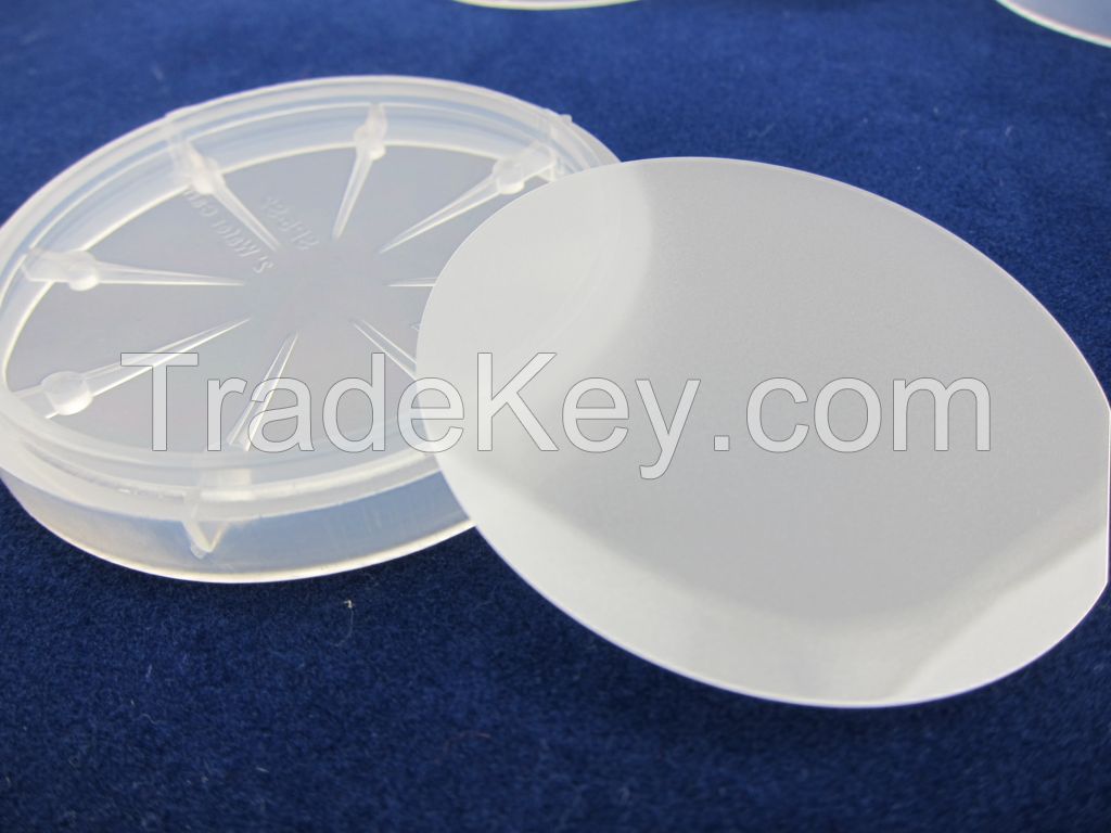
Contact Now

Product Description

Applications:

Blue LDs(**5nm < **0_**5nm>) can be used for high-density data storage, laser print, laser display, laser projection camera, etc.
GaN-based MQWs LDs
Short wavelength laser: Green/UV/Deep UV

Specifications:

ItemGaN-FS-N
Dimensions *0.8mm ± 1mm
Marco Defect DensityA Level≤ 2 cm*2
B Level> 2 cm*2
Thickness**0 ± *0 μ M
OrientationC-axis(***1) ± 0.5°
Orientation Flat(****0) ± 0.5° , *8.0 ± 1.0mm
Secondary Orientation Flat(****0) ± 3° , 9.0 ± 1.0mm
TTV(Total Thickness Variation)≤ *5 μ M
BOW≤ *0 μ M


Conduction TypeN-type
Resistivity(**0K)< 0.5 Ω@********************"color: rgb(*4, *4, *4); font-family: Arial, Verdana, sans-serif; font-size: *2px; line-height: normal;"> Dislocation DensityLess than 5X**6 cm*2
Useable Surface Area> *0%
PolishingFront Surface: Ra < 0.5nm. Epi-ready polished
Back Surface: 1. Fine ground, Ra < *0nm, 2. Rough grinded
PackagePackaged in a class **0 clean room environment, in single wafer containers, under a nitrogen atmosphere.

Item GaN-FS-N GaN-FS-SI
Dimensions *0.8mm ± 1mm
Thickness **0 ± *5 µm
Useable Surface Area LD Level > *0%
LED Level > *8%
Orientation C-axis(***1) ± 0.5°
Orientation Flat (****0) ± 0.5°, *6.0 ± 1.0mm
Secondary Orientation Flat (****0) ± 3°, 8.0 ± 1.0mm
TTV(Total Thickness Variation) ≤*5 µm
BOW ≤*0 µm
Conduction Type N-type Semi-Insulating
Resistivity(**0K) < 0.5 Ω

Country: China
Model No: -
FOB Price: Get Latest Price
Place of Origin: -
Price for Minimum Order: -
Minimum Order Quantity: -
Packaging Detail: -
Delivery Time: -
Supplying Ability: -
Payment Type: -
Product Group : -

Send a direct inquiry to this supplier

To:

Yao < Suzhou Nanowin Science and Technology Co., Ltd >

I want to know: