Please enter full name.
Please enter product name.
Select Industry.
Email address already exists
Please enter Password.
Enter Conatct number.
Please enter company name.
Please enter date.
Enter Message
By Signing Up. I agree to TradeKey.com Terms of Use, Privacy Policy, IPR and receive emails related to our services
Thank you, your message has been sent.
Invalid Email.
Room 318-326, Block H, Zhigu Science park,Shenzhen,Guangdong,China China
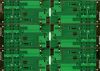
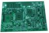
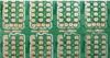
3 HDI / 3 steps HDI board / Layers 14 / Thickness 1.550.15mm / Min. Hole Size 0.1 /0.1mm / Trac
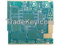
/ High-layercount Multilayers Board / Layers:38 / Thickness:5.00.45mm / Min. Hole Size:0.45mm / T
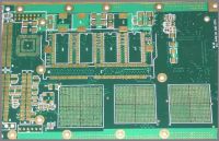
/ Rigid-flex Board / Layers: 12L / Thickness:1.60.15mm / Min. Hole Size:0.2mm / Trace width /
/ Embedded Capacitance Board / Layers 20 / Thickness 2.10.20mm / Min. Hole Size 0.25mm / T
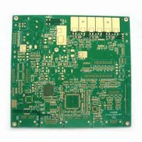
Layers: 18 Thickness: 2.0+/-0.2mm Surface Treatment: ENIG Craft 4 steps unidirectional adding layer stacked hole HDI laser drilling technology, mi
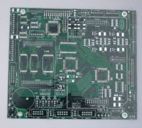
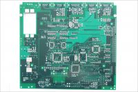
Layers: 6 Thickness: 1.6+/-0.15mm Surface Treatment: ENIG+gold finger Craft EMC EM-370 HF material Application High frequency equipment
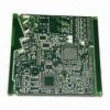
Layers: 4 Thickness: 1.6+/-0.15mm Surface Treatment: ENIG Craft Layers: 4 Application Industry control
Rigid board; 1-48L HDI: 4-48L Rigid-flex/flex: 1-12L Certificate:ISO 9001:2008, US & Canada UL certificates E466113, TS 16949 & RoHS compliance Materi
Shenzhen Yaxinda Technology Co., Ltd established in 2007. As a leading PCB enterprise through 10 years effort, we have two modernization factories in
Contact Person Mr. Harris Liu
Address Room 318-326, Block H, Zhigu Science park, Shenzhen, Guangdong
We will contact you soon .
Please select at least one Buyer/Supplier.
Please enter name.
Please select industry.
Enter Password
Please select country.
Please select state.
Please select city.
Please Enter Message.